Chiplet Shift Reshapes AI Hardware Design, Forcing EDA Reinvention
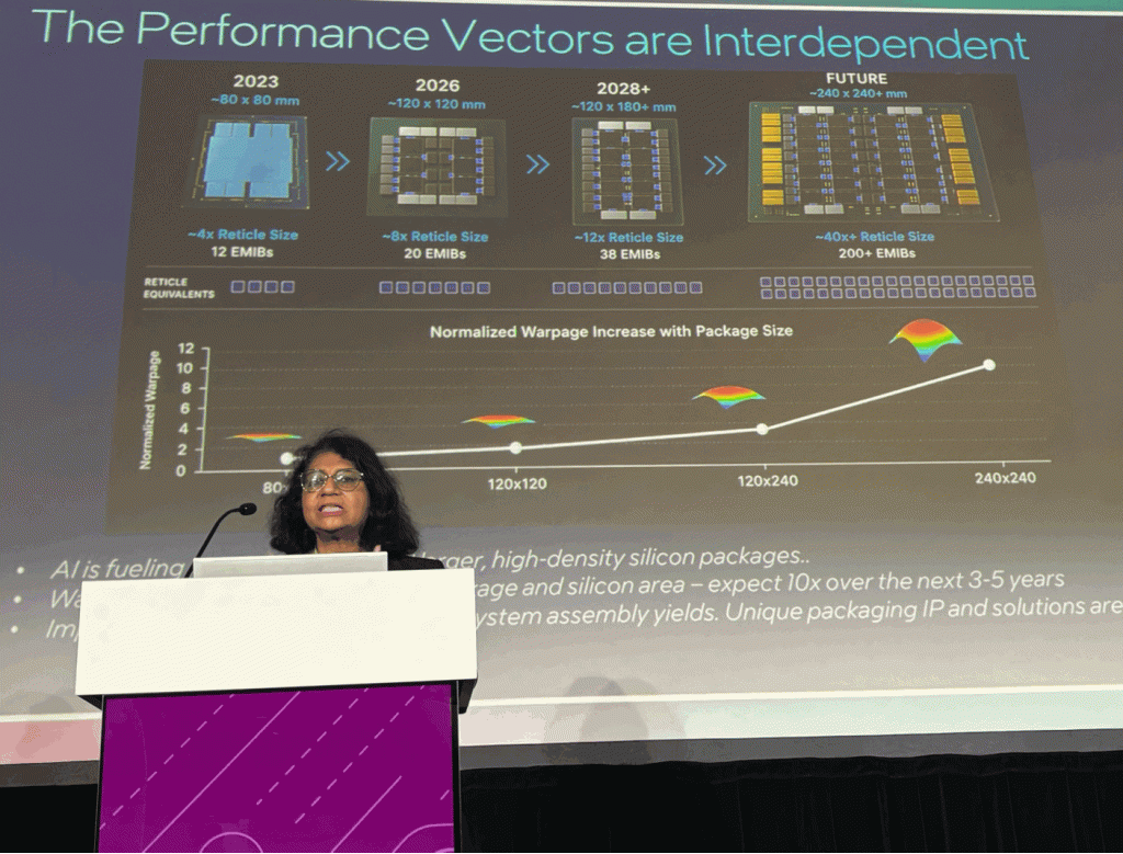
The semiconductor industry's pivot to 3D, chiplet-based architectures for AI hardware is forcing a fundamental reinvention of the Electronic Design Automation (EDA) market. This isn't merely an incremental upgrade; it's a disruptive shift away from monolithic chip design that profoundly alters the economics of silicon. As companies like Intel with its Ponte Vecchio and AMD with its MI300 series validate the performance of stacked designs, the pressure escalates on EDA leaders—Synopsys, Cadence, and Siemens EDA—to deliver tools that can manage the immense complexity of these new systems, moving beyond isolated, 2D verification. The transition to 3D architectures creates clear winners and losers. Fabless AI chip startups gain an asymmetric advantage, able to mix-and-match best-in-class chiplets from different vendors or foundries, drastically lowering NRE costs and time-to-market. This exposes a vulnerability in vertically integrated players who rely on monolithic designs. The EDA vendors themselves are forced into a strategic recalculation, racing to integrate multi-physics analysis (thermal, power, signal integrity) across entire packages, not just single dies. Cadence’s Integrity 3D-IC platform, for example, directly targets this systemic complexity, a far cry from traditional place-and-route tools. Looking forward, the integration of agentic AI into the EDA workflow itself is the most critical variable. Within 12-18 months, expect EDA tools to move from co-pilots to autonomous agents capable of exploring the vast design space of chiplet combinations to optimize for specific AI workloads. This trajectory suggests the basis of competition will shift from tool speed to the sophistication of the embedded AI. The real test will be whether these AI-driven tools can consistently produce designs that outperform human-led efforts, potentially creating a new class of "generatively designed" hardware by 2026.